this post was submitted on 26 Aug 2024
82 points (94.6% liked)
Technology
72690 readers
1799 users here now
This is a most excellent place for technology news and articles.
Our Rules
- Follow the lemmy.world rules.
- Only tech related news or articles.
- Be excellent to each other!
- Mod approved content bots can post up to 10 articles per day.
- Threads asking for personal tech support may be deleted.
- Politics threads may be removed.
- No memes allowed as posts, OK to post as comments.
- Only approved bots from the list below, this includes using AI responses and summaries. To ask if your bot can be added please contact a mod.
- Check for duplicates before posting, duplicates may be removed
- Accounts 7 days and younger will have their posts automatically removed.
Approved Bots
founded 2 years ago
MODERATORS
you are viewing a single comment's thread
view the rest of the comments
view the rest of the comments

A+E will work in E. It's more on the motherboard manufacturer if it's supported or not. Check your manual.
Thanks! Can you elaborate on what would cause it to not be supported? I know the wifi card I'm replacing is an e-key, and I'm using a laptop so I likely won't find any information. Also, if you would happen to know what brands I should look out for that have good linux compatibility if I want to buy a newer one?
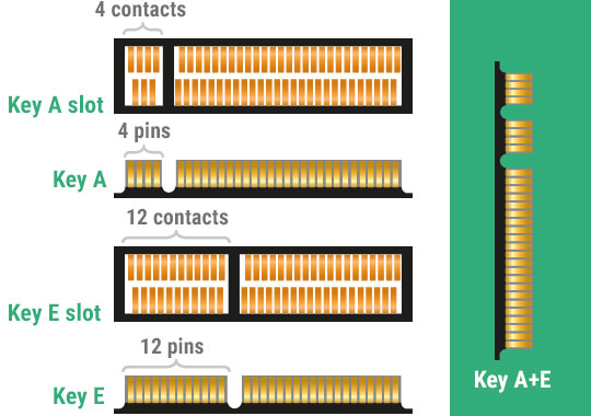
Be very wary of the staggered pins in the diagram. I don't trust the diagram.
Thank you for your input! I can't tell if the diagram was made poorly or if M.2 does use staggered pins.
I'm not entirely sure myself with current tech, but when we got our first external adapter for SSD drives for MacBooks, the connector was made so sloppy that you'd literally have to manually make sure it was aligned properly in the slot.
There was like half a millimeter of slop in the slot where if you inserted it incorrectly, everything would lose its magic smoke..
You seem to love spreading misinformation on the web. Why are you commenting 4 times if you are not familiar with the topic?
This is an m.2 connector. You have to secure it with a screw on the other side. It's nearly impossible to mess it up.
Apple frequently uses proprietary connectors, I don't know which one you are reffering to. I won't guess because I'm not very familiar with all apple connectors.
You don't have to comment on a topic if you are not familiar with. Please stop.
Why is the diagram incomplete? It shows both sides of the socket, but only one side of the card. Are the pins really staggered like that?
I never trust incomplete diagrams, and I'm not finding a proper diagram that shows both sides to confirm or deny anything.
It's a strange diagram but shows what you have to know. If you ever seen different keyed m.2 cards, you should understand this. The important thing is the location of the keys, the notch. All m.2 cards has an 'up' and 'down' side, it shows only the 'up' side. You have to look inside the receptor to see the pins, that's why it shows both sides, it's not possible to see one side only on the receptor as they are in a plastic casing. Usually you can't see the pins on the mobo, only the key.
You can see a similar diagram on wikipedia, both sides of receptor, top side of card:
The offset you were writing about doesn't matter, it actually helps. You can't accidentally insert the card upside down. The location of notches also help with this, as not all possible notches used yet, but in the future it could change.
These connectors are really small. The receptor is similar how sodimm connector works, but smaller. Are you also afraid about inserting a ram in an laptop? It's basically the same.
Read more about the connector in wikipedia, I'm really happy this slowly replaces sata, msata, mpcie and even pcie in current pcs.
https://en.wikipedia.org/wiki/M.2
Did you not notice the staggered pinout on the diagram? That looks like it's literally designed to be a short circuit no matter what the manual says.
I've literally dealt with staggered pin short circuits twice in my life, one from equipment damage, and another from piss poor engineering.
Either way it'll totally fry the power supply, if not more..
I thought the staggered contacts engage with similarly staggered pins on the other side of the card?? 🤔
You are right. The user you are replying to has no idea what they write about, as they confessed in another comment.
I'm not hands on familiar with these standards, so I'm not entirely sure. But when I see a diagram showing 4 pins on one side and 3 pins on the other, but the card going into it only shows one side, then it raises immediate red flags of incomplete information.
No worries, my card has 4 on one side and 3 on the other, so I don't believe that will be an issue. I thought that you were more concerned about the slight difference in the pin's location from top to bottom of the slot diagram.
Cool cool. I was worried that it might be a piss poor diagram made by a 10 year old just learning Photoshop or something.
When it comes to electronic diagrams, I'm used to seeing complete pinouts that label every single pin, like ground, power, data and clock signals and whatnot.
Seeing such an incomplete diagram like this one just scares me though.